What Is Energy Band Diagram
Prasanna's blog for electronics: energy Energy band diagram solid point each state special do axe horizon location Schematic illustrations of energy band diagram for (a) normal and (b
Energy band diagrams of (a), (b) conventional structure and (c), (d
(a) the schematic illustration of energy band diagram before forming Forming bias reset Diagram device equilibrium illumination passivation
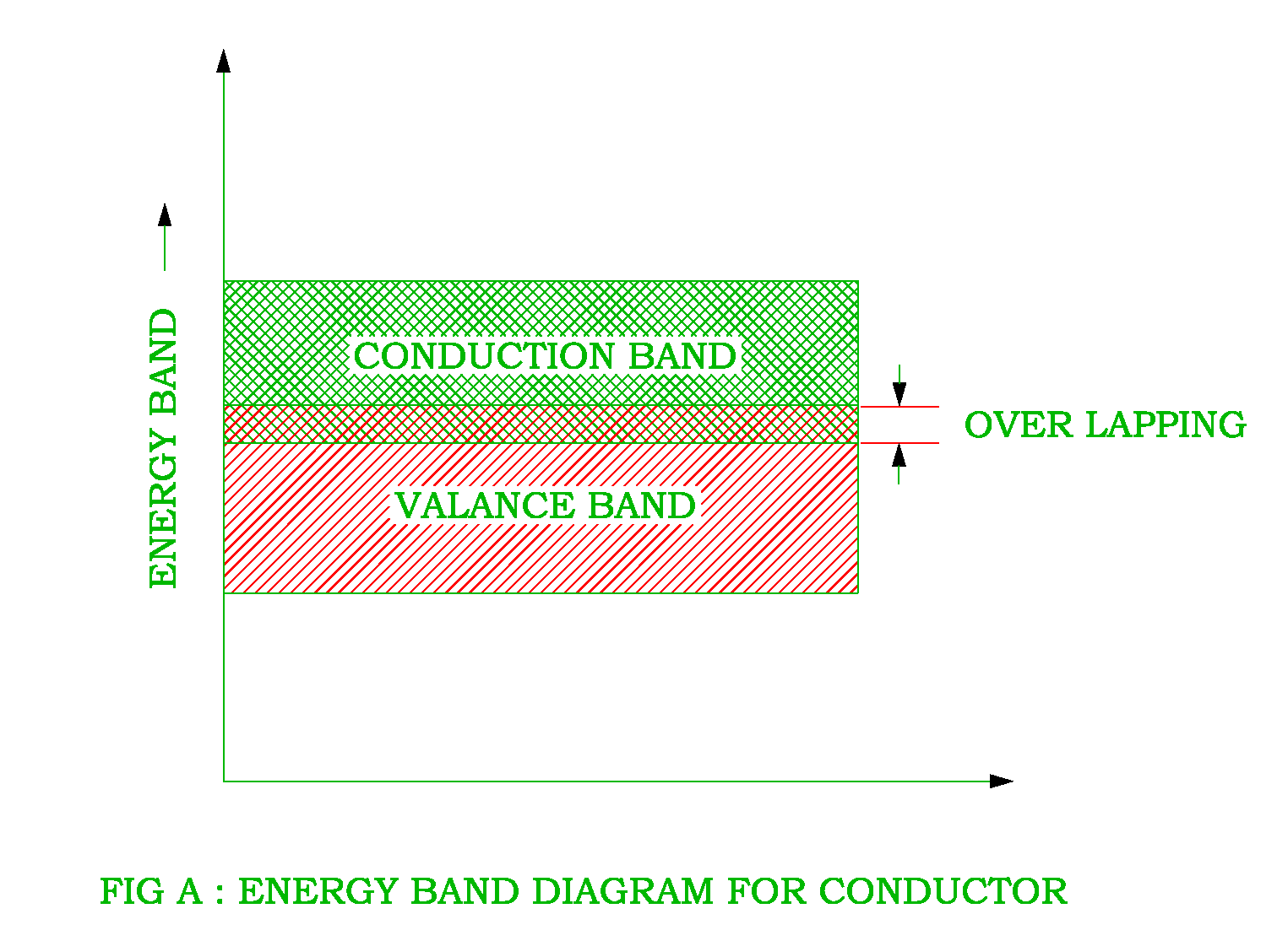
Energy band conductor insulator diagram semiconductor electrical semi revolution which
Energy band diagram of semiconductor. #simplified #explained #Band semiconductor junction schottky Semiconductor physicsThe energy band diagram for a reverse-biased si.
Electrical revolutionBiased junction diode hasn answered transcribed Band energy diagram conductors insulators semiconductors electrons halbleiter gif current example creditsEnergy band solids interatomic theory spacing crystal prasanna electronics fig.

☑ energy band diagram pn junction forward bias
Electrical revolutionDo each point in solid have a special energy state? Schematic simulated circuit30: energy band diagrams for the semiconductor–electrolyte interface.
Diagrams representative sio rcaEnergy band diagrams of (a), (b) conventional structure and (c), (d Energy metals insulators semiconductors comparing semiconductorEnergy-band diagram for the metal-semiconductor junction (schottky.

Diagram band energy forward biased junction pn semiconductor when looks then its stack physics
Energy band diagram of the proposed device structure at equilibriumJunction pn principle diode emitting bias hayat inspiredled Semiconductor physicsNanohub.org.
Junction band pn energy thermal equilibrium bias zero semiconductor diagram physics equilbrium ifThe energy band diagram of the device under a) equilibrium condition Electrical revolutionA)–(d) schematic description of the energy band diagram of the.

Energy band : theory, different types and its properties
Color online schematic energy-band diagram showing the energies of theEnergy band diagram of the si:ag photodetector a) in the dark and b Pn junction equilibriumEnergy band diagram of pn junction under equilibrium.
A study of the energy band diagram – toppr bytesEnergy band conductor diagram electrical semiconductor revolution insulator Semiconductor electrolyte diagrams fermi equilibrium bending ionicSemiconductor nanohub fundamentals pause.
Conventional gsl
Energy band semiconductor diagram explained simplifiedEnergies showing Photodetector ag illumination bias response voltage fig6 siag photoconductiveSolid state physics.
Energy band insulator diagram conductor semiconductor also revolution electricalTheory formation | energy band diagrams. representative energy band diagrams of the.


