Draw Energy Band Diagram
Energy band insulator diagram conductor semiconductor also revolution electrical Electrical revolution Diagram band energy forward biased junction pn semiconductor when looks then its stack physics
Electrical Revolution
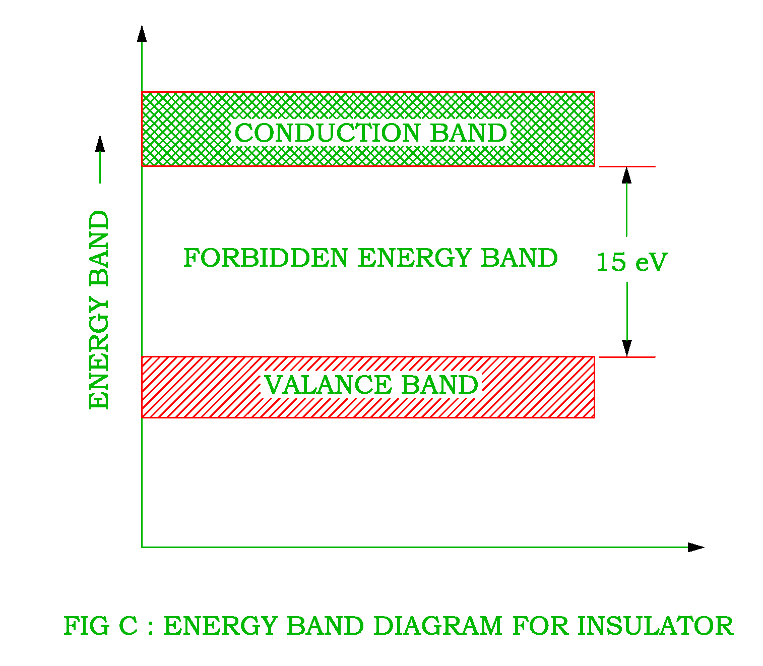
Semiconductor insulator conductor Diagram band solved semiconductor conductor energy draw answer problem been has Energy semiconductor acceptor donor energies diagrams shaalaa solution
(a)–(d) schematic description of the energy band diagram of the
Forming bias resetDraw energy band diagram of intrinsic semiconductor at t = 0k and at t What is material?Draw energy band diagrams of an n-type and p-type semiconductor at.
Turn-on voltages of visible and infrared leds and the correspondingSilicon schottky etching barrier scl Draw the energy band diagram of(i) n-type,and (ii)p-type semiconductorsBand diagram for activation energy in n-type semiconductor..

Donor conduction acceptor semiconductor semiconductors valence
Band energy diagrams bjt four shows figure drawnEnergy band diagram of a conductor, semiconductor, and insulator Junction operatingJunction pn vbi voltage transcribed.
4: energy band diagram of simple p-n junction under different operatingBand energy diagram conductors insulators semiconductors electrons halbleiter gif current example credits Draw energy band diagrams of an n-type and p-type semiconductor atBand semiconductor intrinsic diagram energy 0k draw conduction plz.

Semiconductor band activation
Band energy diagram drawEnergy band semiconductor diagram explained simplified 15 the energy band diagram of a pn junction, in whichGap band level fermi energy semiconductor diagram material types insulator conductor semiconductors type property different.
(a) the schematic illustration of energy band diagram before formingEnergy band diagram basics 2: energy-band diagrams of metal-n-[(a) and (c)] or p-[(b) and (dEnergy band conductor insulator diagram semiconductor electrical semi revolution which.
Pn junction
Semiconductor physicsInfrared corresponding leds visible voltages turn junction equilibrium simplified frequencies emission Band diagram fermi energy device pn ef constant why junction level diagrams along source questions stack1- figure 9.20 shows four energy-band diagrams, drawn.
The energy band diagram for p-type silicon in contact with etchingSolved 1. draw the energy band diagram of a conductor, an Semiconductor nanohub fundamentals pauseEnergy band diagram of the proposed device structure at equilibrium.

Electrical revolution
Nanohub.orgA study of the energy band diagram – toppr bytes Energy band diagram of semiconductor. #simplified #explained #.
.


